Tear-Down of an HP ProCurve 2824 Ethernet Switch

One of the courses I’m taking this quarter at Cal Poly is an Introduction to Computer Networks course, where we learn about the 7 layer OSI model, and then learn about how networking works from the bottom up. Like most Cal Poly classes, this includes a lab, where we take a bunch of Ethernet cables and Cisco gear (thanks Cisco!) and run around for a few hours to hopefully learn something.
The lab this previous week was an interesting one where we had 1,000 (virtual) devices all send traffic at a network switch all at once, and see how quickly and intelligently the switch can process all of this traffic. Moving packets between the Ethernet ports was no issue for the switch, but where it choked was processing Ethernet frames from devices it had never seen before. While any decent network switch can move a couple million packets between physical ports, when a new MAC address passes through a switch on the network it needs to do a little more processing to remember where this MAC address came from. This “MAC Address Learning” is a nice feature of switches, such that they only send traffic down the single link towards it’s destination instead of all four, eight, 24, or 48 ports connected to the switch. This greatly multiplies the effective throughput of any switched network by freeing up the bandwidth of every other link to do other useful work.
Long story short, while a switch can move millions of packets, it can only learn a few thousand new MAC addresses per second. This isn’t particularly important, since having more than maybe one or two dozen MAC addresses on one L2 home network is rare, and even in a large network you won’t see thousands of MAC addresses join or physically move in the network in a second.
I also happen to be the only EE in this CPE/CSC class, which even with 60 students is evident to the point where the professor has opted to call me “the EE guy” in lieu of learning my name. This lab piqued my interest in the internals of a network switch and why it can switch frames orders of magnitude faster than it can process them, so since I’m the only person in the classes who soils himself with physical hardware, I figured I should tear one apart and see what an Ethernet switch looks like.

Of course, the Cal Poly CPE department would probably be pretty displeased if I went into the networks lab with a screw driver and went to town in one of their switches. Luckily, I have a level 60 junk box with a +5 against finding random electronics, so I just so happen to have a spare HP ProCurve 24 port Gigabit Ethernet switch sitting in my closet.

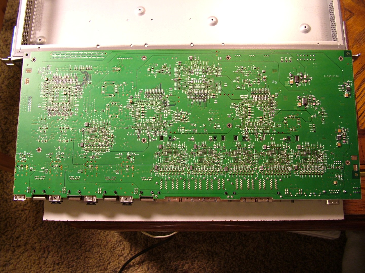
Starting with a bird-eye view of the switch’s entire motherboard, the system can be roughly divided into three sections. (Note: all of these pictures can be clicked on to see much larger versions, and I’m including both the diagrammed and unmolested versions of the pictures, for your enjoyment.)
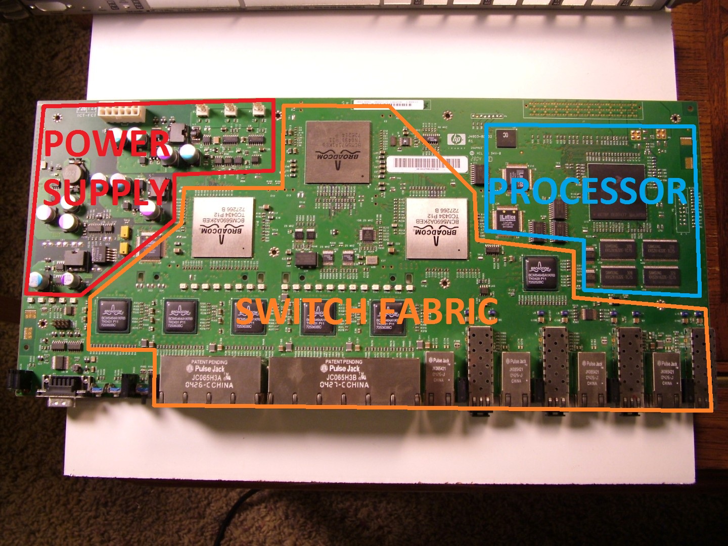
- In red on the top left of the board is the switching power supply, which takes 12V from a 120VAC power supply and converts it down to the high current low voltage (3.3V) needed by all the ICs.
- Boxed in blue on the top right is the actual processor of the switch, in addition to the supporting RAM and Flash memory. The switch's operating system runs on this processor, and is thus what you interact with to change settings on the switch.
- The giant orange region, which takes up most of the board's area, is the hierarchical switching hardware, which operates as an independent system from the processor to switch Ethernet frames from one port to another.
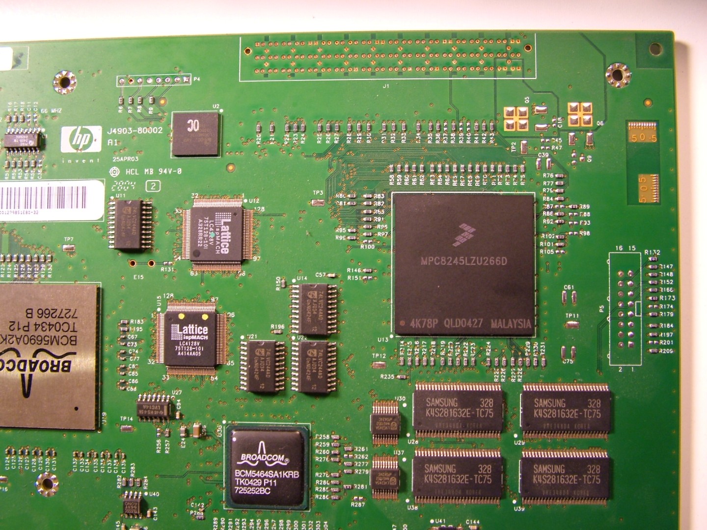
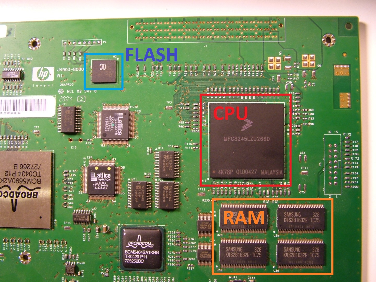
- CPU: MPC8245LZU266D (boxed in red) - [Freescale product] [Mouser] This. This is why network switches can't process Ethernet frames very fast. This 24-port Gigabit switch runs off of a deeply-underwhelming 266MHz PowerPC processor. The fastest IO port on this processor is a PCI bus, which can barely push 250-500Mb through a NIC (Fun fact: this is why PCI 1000bT NICs are pointless, and why 1000bT really needs PCI-X or PCIe to do much good). Luckily, as we'll see, this PCI bus is useful since it is how the CPU communicates with and configures the switch fabric, but appreciate that this bus is orders of magnitude slower than the network traffic handled by the switch. The only thing going through the PCI bus is configuration settings, individual Ethernet frames extracted for analysis, and network traffic directed at this switch's operating system.
- RAM: 4x K4S281632 (orange) - Each IC contains 128Mb of SRAM, giving the switch a whopping 64MB of RAM. Since hardware like this switch enjoys the benefit of having a very specific purpose in life, it doesn't need the GBs of RAM needed in general purpose computers, and 64MB is plenty to run the switch's simple OS.
- Flash ROM: AMD L065 (blue) - A 64Mb (8MB) flash chip that is used to store the switch's operating system image and configuration data. This is why the first thing you see on the terminal when you turn on a network switch is something like "Uncompressing Operating System Image..."; 8MB may be enough to store everything needed for the switch, but just barely. One thing that is kind of neat about this part, since it was manufactured by AMD (which spun-off into Spansion), is that at some point during development it crossed my father's desk on it's way to the foundry. One of the joys of growing up in the Silicon Valley; you probably have an IC in your pocket that helped fund my childhood.
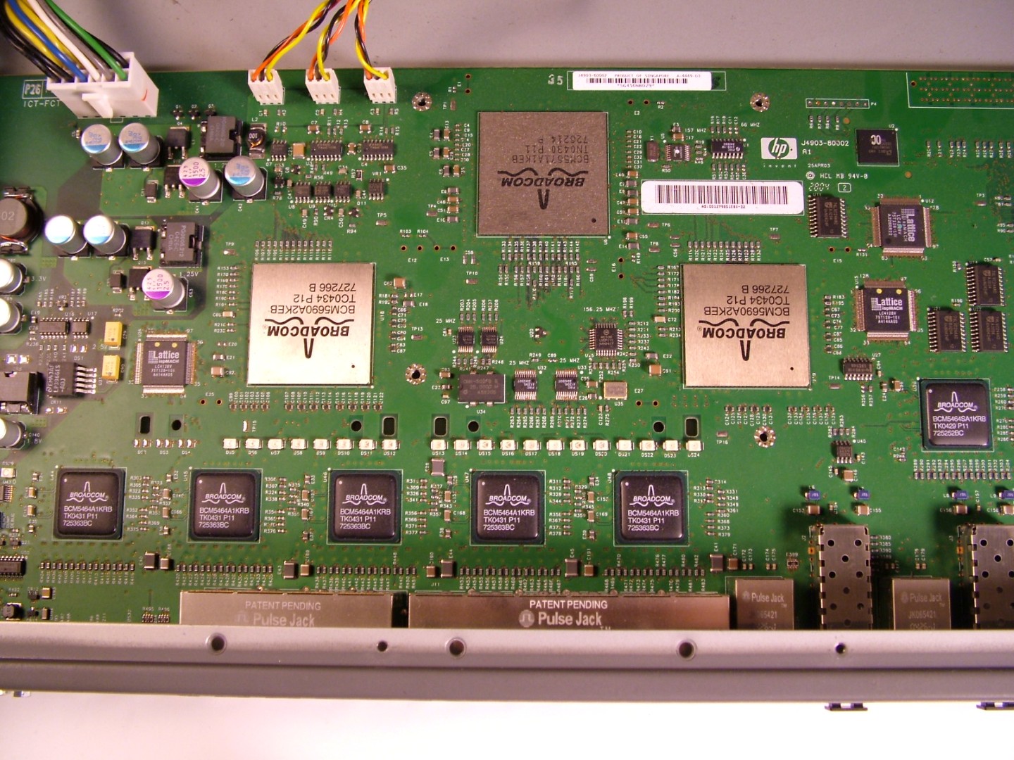
- The Ethernet transceivers along the bottom to translate magnetic pulses from CAT5E/6 or light pulses from fiber optic Ethernet cables into digital signals to be processed inside the switch.
- Multiple 1Gb switches, which each support a finite number of external ports, and have a single, faster, uplink port.
- A crazy fast 10Gb switch, which handles passing traffic between the 1Gb switches if a frame doesn't happen to be able to be switched internally to a single 1Gb switch. This forms a hierarchical format that allows the same ICs to be used to build different switches ranging in size from a few ports up to a LOT of ports (48 in the case of a single top-level 10Gb switching fabric ASIC, 384 ports theoretically).
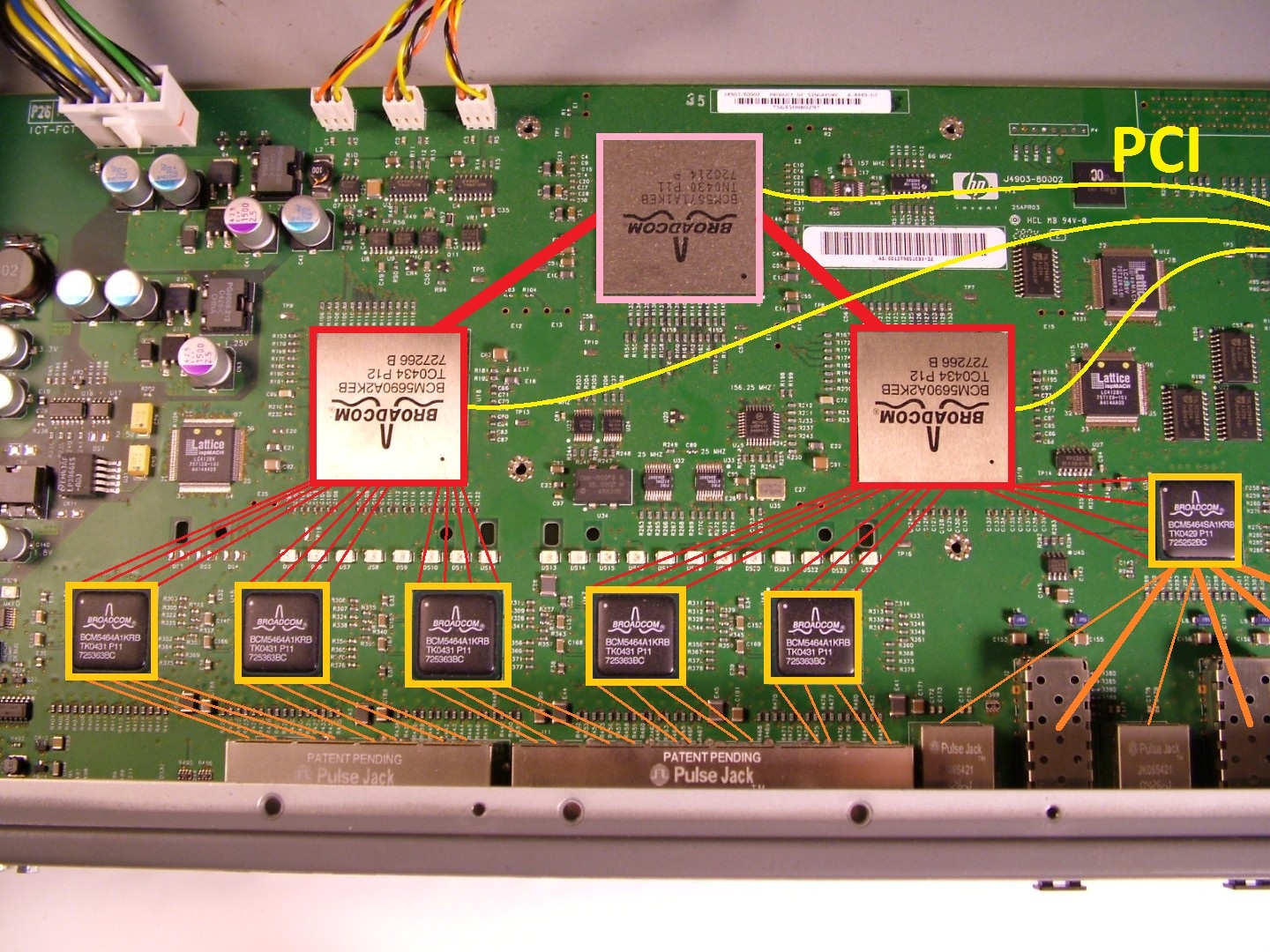
- Physical transceivers ( boxed in mustard): 5x BCM5464A1KRB, 1x BCM5464SA1KRB - [Broadcom product] The physical transceivers are decoupled from the switching ICs, since while most Ethernet is 802.3 twisted pair, there are other physical mediums which are still Ethernet, so Broadcom wants to be able to support using the same switching ICs regardless of what physical layer is used. This is enabled by the GMII bus, which allows any standard MAC device (such as the switch ASICs) to interact with any Gigabit PHY transceiver (such as twisted pair or fiber optic transceivers).
- The main 20 ports of this switch are served by five quad transceivers, which each have four GMII ports and Ethernet transmitters and receivers sets for four distinct links.
- The four "dual personality" ports on the right (only two shown in frame) use a slightly different transceiver, since each port supports using either the internal 1000BASE-T transceiver or plugging a different transceiver into the adjacent SFP or "mini-GBIC" port. The standard BASE-T Ethernet over unshielded twisted pair that you always see is only rated for link lengths of 100 meters. This is perfectly fine between anywhere in your house, and usually even between any two places in a single building, but once you're constructing a network to cover an organization's entire campus or something larger, you find you need links longer than 100m, which is where fiber Ethernet is used. There are multiple different types of fiber optic cables and optical transceivers, so I've never seen a switch that doesn't support interchangeable SFP or GBIC modules, so that the network administrator can select the best transceiver for the application.
- 12 port Gigabit Switch (red): 2x BCM5690 - [Broadcom product] These ICs are specially made to do almost nothing but be really really good at switching frames between 12 Ethernet ports really fast, where each port is connected through a GMII bus to a PHY transceiver (or in this case, three quad transceivers).
- These switching ICs have a surprising amount of intelligence internal to them. Configured via it's PCI port or a static EEPROM, the switching IC maintains various state such as where to route frames addressed to specific MAC addresses, how to interpret quality of service and VLAN tags in Ethernet frames, etc, without processor intervention. This is why it's acceptable to use a bus as painfully slow as PCI between the switch ASICs and the switch's processor. It's also why unmanaged switches can loaf along with no processor at all, making do with one of these switch ASICs, some number of PHY transceivers connected to it, and a configuration EEPROM.
- If an Ethernet frame comes in one port and happens to only need to leave via another port on the same BCM5690 switch, all is well, it's switched, and life goes on. On the other hand, if a frame needs to be sent out ports not directly connected to the 12 ports of this switch, they need to be passed to the correct BCM5690. This is done via a 10Gb XAUI bus port which supplements the 12 GMII ports. XAUI is an extension to the 10Gb XGMII bus (which is the 10Gb variant of MII) which allows the XAUI bus to be routed up to 50cm between the MAC & PHY, where XGMII is limited to 7cm. (Was that enough alphabet soup for you?) Long story short, it's a 10Gb link capable of reaching from one end of the switch's motherboard to the other, to connect multiple 12 port switching ASICs.
- 4 port XAUI Switch Fabric (pink): BCM5671 - [Broadcom product] When you have more than one BCM5690 switch, you need some way to tie them together via their XAUI buses to pass traffic back and forth.
- From what information I can find online, it appears that it is possible to connect two BCM5690s back-to-back using their XAUI ports, so it's not entirely clear to me why HP's ProCurve 2824 uses a four port Switch Fabric to connect only two switches together. The best I can come up with is that they wanted the internal architecture to be as close as possible to the higher end ProCurve 2848, which is the network switch from the same product line with twice as many ports.
- One thing to note is that these XAUI links between the switches and switch fabric are 10Gb in each direction. This is really freaking fast, but is less than the theoretical throughput of each BCM5690 end-point. The chances of all 12 Gigabit ports on one half of this switch saturating with traffic for the other half is remote, but it is academically possible to expose the 10Gb limitation between the two halves of the switch hierarchy. The chances of this happening are ridiculously slim, and if this was a protracted issue, it would probably indicate poor network design more than a limitation of this hardware.
- I gather that the switching fabric can support as many as 32 BCM5690 end points, which translates to 384 Gb ports. Switches larger than 48 ports would likely use larger switch fabrics with more than four XAUI ports, but eventually connections would probably need to be made between multiple switch fabrics.
- The rows of capacitors lining the edges of each IC for power supply filtering. These ICs all draw so much power so quickly that the inductance between the power supply and each IC can become problematic without local filtering.
- The fact that the ground plane isn't one continuous copper pour from edge to edge, but is tactically partitioned between various sub-systems. This helps to reduce interference between ICs, and reduces the amount of EMI emitted from the system as a whole.